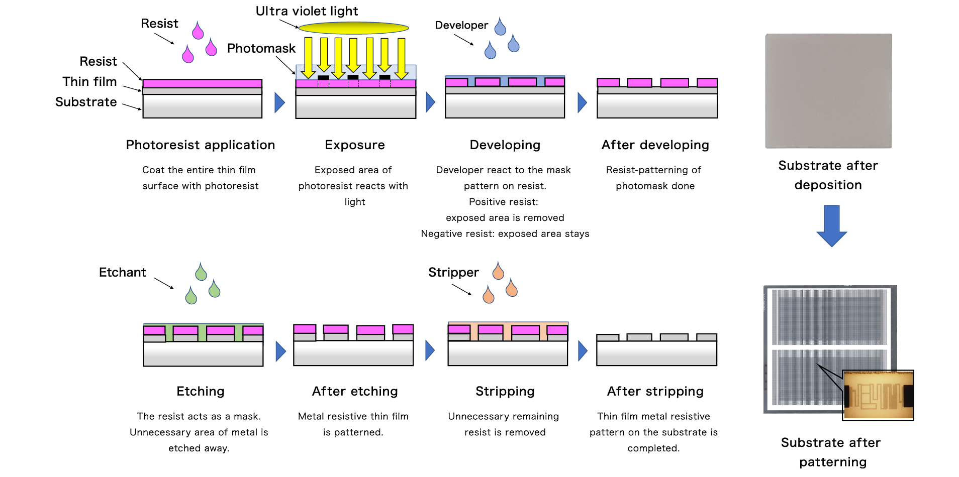
■ Susumu's thin film deposition technologies such as sputtering and plasma CDV create a high quality homogeneous resistive film and a superb environmental protective cover, which materializes high reliability and stability.
■ Current runs though evenly and smoothly, which helps attain long-term stability.
Features
・High precision and small TCR
・Current density is distributed evenly. Stable performance with minimal resistance drift in time.

Automotive, FA industrial equipment
Susumu offers thin film resistors more tolerant to harsh environment than conventional thin film resistors
Inorganic
passivation
RG series
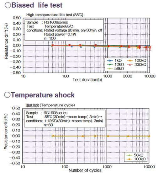
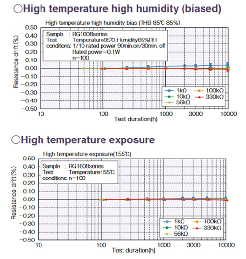
Drift less than±0.1%in all tests, compliant to AEC-Q200
★Resistor noise is generally given by
Noise=thermal noise +current noise(1/f noise)
Thermal noise’s noise effective value is given by

As the formula indicates, thermal noise is decided by temperature, resistance and frequency, s
which means there is no difference by material(same for thin or thick film)。
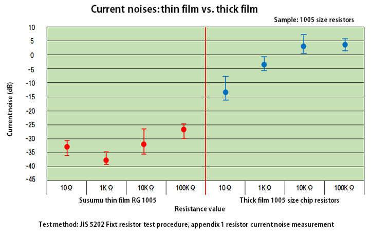
Current noise(1/f noise)is caused by the movement of free electron (carrier) and it appears at lower frequencies, it is dependent of materials and structures. The current noise is much smaller in thin film than thick film (refer to the noise comparison between thin film and thick film)

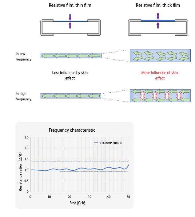
In high frequency, "skin effect" where more electrons moves surface of the conductor takes place. But thin film is only tens of nanometers thick and avoids to have skin effect even in high frequency and resistance stays relatively stable.
"Skin effect" is a phenomenon in which alternate current starts moving mostly on the surface of a conductor and current movement is restricted. The higher the frequency, the stronger the skin effect.
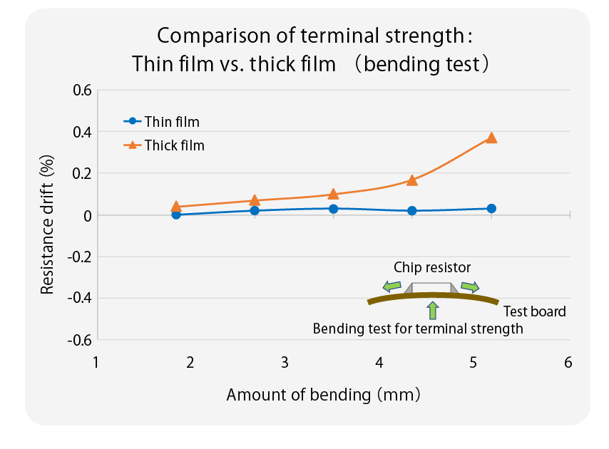
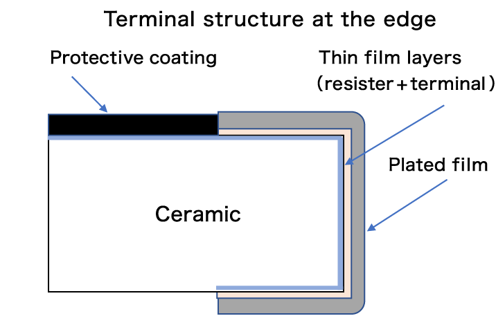
In our thin film resistors, the edges are also metalized by sputtering, which gives strong and stable adhesion between the ceramic and terminal material.
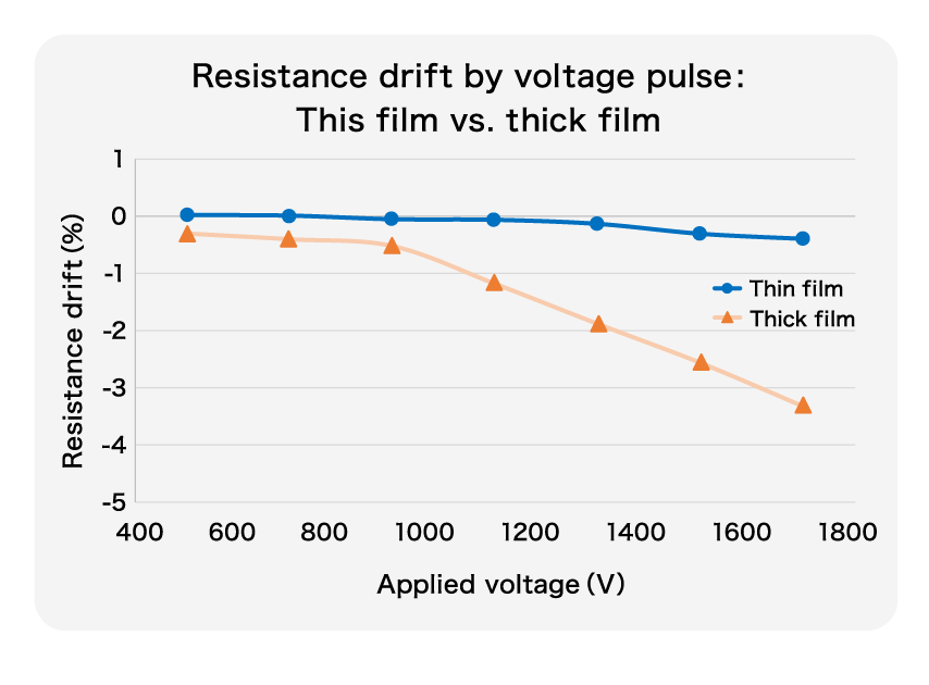
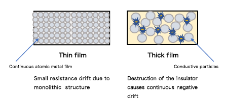
During the thin film metallization,
first atomic nuclei islands form.
These islands grow, connect, and create a continuous film.
This monolithic structure (continuous atomic metal film)
withstands voltage stress and damage resulting
in less resistance drift until the film is destroyed.
Thin film resistors are patterned with photolithography, the same technique used for semiconductors.
Photolithography's capability of creating precise, fine patterns enables us to form small, fine, and intricate resistive patterns.
