|
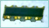
Thin Film Chip Network Resistor |
|
|
Thin Film Chip Network Resistor |
|
| Fine tracking performance even in a combination with different valued resistors |
|
YDS’s
Thin Film Chip Network Resistor has fine tracking performance as well as fine characteristics of high
precision thin film. This chip network resistor is forming thin film by
spattering and resistance value is specified by patterning and high
precision laser trimming. On the same substrate, elements are formed out
of thin film and have the same characteristics as well as the tendency
of change such as tracking resistance temperature coefficient
and heat stress. Therefore it can keep the steady tracking ratio. The tracking
performance can be maintained even in a combination with different
resistors. Various types are available for different powers or in many
ways. Custom requests are also welcomed. It offers amelioration of
circuit performance and cost merits by fewer assembly operations and
fewer components. |
| … Features … |
|
•
• Fine tracking characteristics; typical: tracking resistance error
±0.05% tracking resistance temperature coefficient ±2ppm/°C •
High tracking precision guaranteed even in a combination with other sorts
of resistors •
High precision and stability because of high precision thin film •
•Surface-mounted type with round wrapped electrodes enables to
automatically mount easily; served by taping •
Some of chip network resistors can be faced down in a smaller area. •
•Thin film manufacturing method always offers the constant
characteristics with very small differences within a lot and between lots. •
Served at the reasonable price with fine tracking precision •
Various types are available for different powers and in many ways, and
applied to various circuits.
|
| … Type … |
|
A variety of products such as high density miniature products which can be surface mounted, standard products with wrap-type electrode terminals and high precision and high density resistance alleys which consist of gold-plating concave electrodes are available. Each of them can be designed for the combination of different valued resistors of the custom-made. |
| Type | Size | Terminals | Elements | Resistance Range | Tracking Resistance | Tracking TCR | Terminal Material |
| RA0816 | 0.8×1.6×0.4 | 8 | 4 | 100~30KO | ±0.1% | ±5ppm/°C | Solder |
| RA2020 | 2.0×2.0×0.4 | 6 | 3 or 4 | 100~100KO | ±0.1% | ±5ppm/°C | Gold |
| RA1632 | 1.6×3.2×0.4 | 8 | 4 | 50~100KO | ±0.1% | ±5ppm/°C | Gold |
| RA4556 | 4.5×5.6×0.4 | 8 | 4 | 50~200KO | ±0.1% | ±5ppm/°C | Gold |
| RN1220 | 1.25×2.0×0.4 | 3 or 4 | 2 or 3 | 50~20KO | ±0.1% | ±5ppm/°C | Solder |
| RN1632 | 1.6×3.2×0.4 | 3 or 4 | 2 or 3 | 50~100KO | ±0.1% | ±5ppm/°C | Solder |
| RN4556 | 4.5×5.6×0.4 | 3 or 4 | 2 or 3 | 50~200KO | ±0.1% | ±5ppm/°C | Solder |
| … Tracking Performance of Thin Chip Network Resistor … |
|
In
a circuit where precision of tracking ratio is required, there seems to
be many cases when each of resistors is required to have fine absolute
precision. For instance, when 0.2% of tracking resistance ratio is
required, it is necessary to put resistor with ±0.1%
of absolute precision. Also, about temperature coefficient of
resistance, when 10ppm/°C is required, it is necessary to put resistor
with ±5ppm/°C.
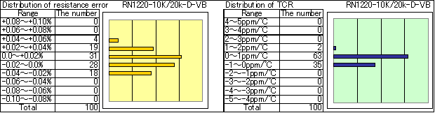
Tracking performance in a network is very fine because YDS’s thin film
chip network is manufactured with technology which can form thin film
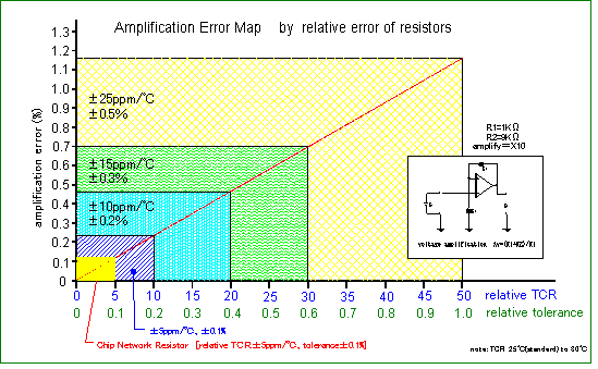
resistors at a time on the same substrate. The comparison of the network
and the error generated in a combination with resistors in the amplified
circuit is showed in the right figure. The standard tracking performance
data is showed in the below. |
|
|
|
|
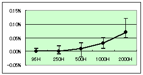
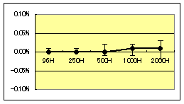
| On YDS’s thin film chip network, resistors are formed at a time and processed under the same condition, so it has a characteristic without any change of the stress and the resistance ratio. Even if the stress and time make a change of absolute value, it will make little change of relative value. The data of absolute value and relative in a long life test at the temperature of 70°C are showed. |
|
Absolute Change |
Tracking Change |
|
|
|
<Detailed Information>
For further information of RN CLICK!
For further information of RA CLICK!
<Taping>
For further information of Taping CLICK!
|
Yokohama Densi Seiko Co., Ltd. |