| RA1632 | ||
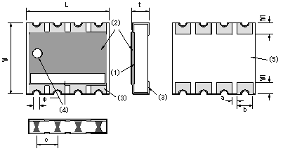 |
Dimension( mm) | |
| L | 3.2±0.2 | |
| W | 1.6±0.2 | |
| t | 0.5±0.2 | |
| a | (0.2) | |
| b | 0.6±0.1 | |
| c | 0.8±0.1 | |
| W1 | 0.4±0.2 | |
| f | 0.3 | |
|
Chip Network Resistor RA series |
?
?
| RA1632 | ||
|
Dimension( mm) | |
| L | 3.2±0.2 | |
| W | 1.6±0.2 | |
| t | 0.5±0.2 | |
| a | (0.2) | |
| b | 0.6±0.1 | |
| c | 0.8±0.1 | |
| W1 | 0.4±0.2 | |
| f | 0.3 | |
| RA2020 RA2525 | |||
| Dimension (mm) | |||
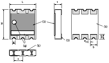 |
RA2020 | RA2525 | |
| L | 2.0±0.2 | 2.54±0.2 | |
| W | 2.0±0.2 | 2.54±0.2 | |
| t | 0.5±0.2 | 0.5±0.2 | |
| a | (0.36) | (0.43) | |
| b | 0.36±0.1 | 0.62±0.2 | |
| c | 0.72±0.1 | 0.86±0.1 | |
| W1 | 0.4±0.25 | 0.5±0.25 | |
| f | 0.24 | 0.31 | |
| RA4556 | ||
|
Dimension (mm) | |
| L | 5.6±0.2 | |
| W | 4.5±0.2 | |
| t | 0.5±0.2 | |
| a | (0.55) | |
| b | 0.7±0.1 | |
| c | 1.25 | |
| W1 | 0.8±0.2 | |
| f | 0.4 | |
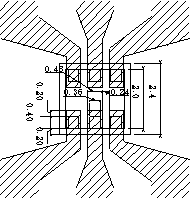
| (1) | Thin Film Resistor |
| (2) | Covering Epoxy |
| (3) | Electrode (Surface soldered and lead free available) |
| (4) | Mark( Dot and bar for the direction) |
| (5) | Alumina substrate |
|
<Equivalent Circuit> |
|
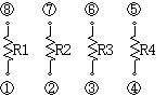
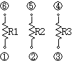
| RA0816?RA1632·RA4556 |
RA2020 RA2525 |
|
|
|
<Specification>
|
Items |
Graph 1 Derating Curve |
||||
| RA1632 | RA2020 | RA2525 | RA4556 | 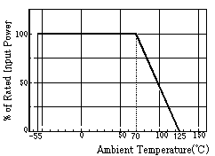 |
|
| Resistance Range | 50~100kO | 100~120kO | 100~180kO | 50~500kO | |
| Resistance Tolerance | ±0.1%·±0.5% | ||||
| Tracking Resistance Tolerance | ±0.1%·±0.2% | ||||
| TCR | ±25ppm/°C | ||||
| Tracking TCR | 5ppm/°C·10ppm/°C | ||||
|
Rated Input Power (Graph1 Derating Curve) |
30mW/element | 42mW/element | 50mW/element | ||
| Operating Temperature Range | -55°C~+125°C | ||||
| Rated Operating Temperature | 70°C | ||||
<Characteristics>
|
Items |
Test Condition |
Tolerance |
|
| Absolute Change | Tracking Change | ||
| Short Time Overload |
2.5 times of the rated voltage shall be applied for 5 seconds. |
±0.1% |
±0.05% |
| Rated Load Life |
Apply rated voltage for 90 min followed by a pause of 30 min at 70±3°C for 1000 hours.70±3°C |
±0.25% |
±0.1% |
| Moisture Load Life |
The Chip Network Resistor is applied rated voltage for 90 min at 60±2°C 90~95%RH for 1000 hours. |
±0.25% |
±0.1% |
| Temperature Cycle |
[-55°C(30min)-R.T.(3min)-+125°C(30min)-R.T.(3min)]
is repeated 5 cycles. |
±0.1% |
±0.05% |
| Soldering Heat Resistance |
Leave NR in melt solder of 260±5°C for 10±1 seconds. |
±0.1% |
±0.05% |
| Strength Between Terminals |
Distance
between fulcrums : 90mm Bending width : 3mm Substrate: Glass epoxy t=1.6mm |
±0.1% |
±0.05% |
| Solderbility |
Leave NR in melt solder of 235±5°C for 3±0.5 seconds. |
95% or more of the surface should be wet. |
|
| Insulation Resistance |
A minute after 500 DC |
1000MO?? | |
|
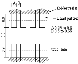
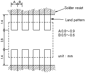
<Recommended
Land> |
|
|
RA1632 |
RA2020 |
|
|
|
|
RA4556 |
|
|
|
|
<Taping>
For further information of packaging CLICK!
|
Yokohama Densi Seiko Co., Ltd. |