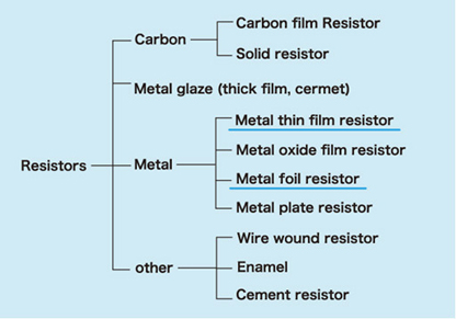
Resistive material
There are numerous resistive materials, Susumu uses the following two materials
Metal thin film →precision thin film chip resistors
Metal foil →current sensing chip resistors
Shapes of resistors
Resistors come in many different shapes. Susumu focus on chip resistors.
Chip resistors
Thin film chip resistors

Thick film resistors

Radial lead resistors

Axial lead resistors

Thin film? How thick is it?
There are many methods to make things thin. Some examples are shown here. Susumu manufactures resistors from thin film using deposition technologies that make film thickness 1um and down to a few Å.

Thin film deposition methods
In electronics, there are many thin film deposition methods. Susumu uses several methods depending on the products and materials. Two main methods, sputtering and plasma assisted chemical vapor deposition are explained here.

Sputtering method
Argon ions, created by glow discharge under vacuum, sputter out target (materials for the thin film) atoms/molecules. These target atoms/molecules adhere to the substrates and form thin film. This method is ideal for depositing metal alloy thin films and high melting point materials.


Plasma assisted Chemical Vapor Deposition (PCVD)
In plasma (glow discharge), thin film precipitate after a series of chemical reaction. Thin film is formed under relatively low temperature. Any materials, organic or inorganic, that can be made into gas compounds can be deposited.


From thin film to resistor
Thin films are deposited with these methods. Thin film technology is not only used for resistors but also used to create internal terminals and protective coating layers.


Please feel free to contact us about products,
requesting documents and samples.


