|
Thermal Variable Attenuator PXV1220S |
|
|
Thermal Variable Attenuator PXV1220S |
|
Easy control of the gain change generated by temperature
change
of high frequency circuit
|
YDS’s Thermal Variable Attenuator is an element, the attenuation of which changes following the change of environmental temperature. If you use this Thermal Variable Attenuator, attenuation decreases as temperature rises, so it can correct characteristics, which lose gain with a temperature rise on the high frequency amplified circuit. With only one Thermal Variable Attenuator, you can directly control input signals with analog continuity and it is the simplest and the most reasonably priced method for adjusting the characteristics influenced by the change of environmental temperature. We can serve not only the improvement of circuit performance but far-reaching merits; cost saving and simplification of material control. We have good results in correcting temperature influences of circuits used in various telecommunication amplifiers for such the base station of cellular phones by using this Thermal Variable Attenuator. |
<Feature>
|
•Fine reproducibility enables attenuation to change to the certain
values following the change of ambient temperatures.
•Analog correcting enables smooth continuous correction by a
single step.
•Due to its simple design, little phase changes and time delay
change by temperature changes
•Available in a wide range from low to high frequency by
consisting of passive resistor materials
•Miniature
size(2.0X1.25mm), light (about 6.5mg) and less area in a circuit
•Easy automatic mounting by surface mount type (served by taping)
•High reliability by simple design and few junctions
•Temperature correction at a more reasonable price than in other
styles
•Using high precision thin film and a special thermostatic
resistor, it makes no attenuation change by effects except temperature,
and guarantees steady operation.
•Serves a
total of 80 temperature correction characteristics. (Each of 10
attenuations has 8 variation slope characteristics.)
|
|
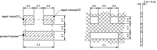
<Mechanical and Dimension> |
||
|
|
||
| A: Mark shows direction, attenuation and slope mark | D: Thermostatic resistor ; Thermistor | |
| B: Protection film; Epoxy resin | E: Thin film resistor | |
| C: Electrode; Solder plated surface, possible to make it lead free | F: Substrate; Alumina | |
|
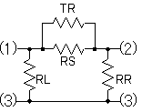
<Equivalent Circuit> |
||
|
|
|
(1),(2) Signal
terminals (3) Ground terminal
|
<Specification>
|
Item |
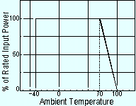
Figure 1 Deratung Curve |
|
|
Attenuation |
|
|
|
Attenuation
Tolerance |
±0.5dB (at 25°C, No-lead) |
|
|
Impedance |
50ohm |
|
| VSWR |
1.3 or less (Ambient Temperature 25°C) |
|
|
Thermo
Sensitive Characteristic |
Each
attenuation has 8 or 9 temperature Characteristics.
Symbol:N1~N8,N9 |
|
|
Frequency
Range |
DC~3GHz |
|
|
Rated
Input Power |
100mW (Figure-1Derating Curve.) |
|
|
Operating
Temperature Range |
-40°C
~+100°C
|
|
|
Rated
Ambient Temperature |
70°C |
|
|
Preservation
Temperature Range |
-45°C~+90°C |
<Characteristics>
|
Item |
Test
Condition |
Tolerance
/ Standard Value |
|
| Short Time Over Load |
2.5
times of the rated voltage shall be applied for 5s. |
±0.1dB |
±1% |
|
Load
life |
Apply rated voltage for 90min followed by a pause of 30min at 70±3°C for 1000H. |
±0.2dB | ±2% |
|
Moisture
Load life |
The attenuator is applied rated voltage for 90min followed by a pause of 30min at 60±2°C and 90~95% RH. This constitutes 1 cycle. Cycles shall be repeated for 1000H. |
±0.2dB | ±2% |
|
Temperature
Cycle |
[-40°C (30min) ~ R.T. (3min) ~ +100°C (30min) ~ R.T. (3min)] is repeated by 5 cycles as one cycle. |
±0.1dB | ±1% |
|
Solder
Heat Resistance |
Leave attenuator floated on the solder tank of for 260±5°C for 10±1seconds. |
±0.1dB |
±1% |
|
Vibration
|
Wave: 10~55Hz, amplitude 1.5mm, sine curve. Sweeping condition: 10-55-10Hz/minute. Added amplitude time: XYZ each 2 hours. |
±0.1dB | ±1% |
|
Solderability |
Leave attenuator floated on the solder tank of 235±5°C for 3±0.5seconds. |
95% or more of the surface should be wet. | |
|
<Recommended
Mounting Pattern> |
|
|
|
Note:
Please take great care of frequency characteristics when deciding the
width of wire from mounted part. |
<Taping>
For further information of packaging CLICK!
<Application>
For further information of the example of use CLICK!
<Data of high frequency characteristics>
|
Yokohama Densi Seiko Co., Ltd. |