| PAT3042 | |||||||
 |
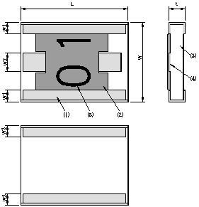
Dimension(mm) | ||||||
| 0dB | 1dB | 2~3dB | 4~6dB | 7~10dB | 16~20dB | ||
| L | 4.2±0.2 | ||||||
| W | 3.0±0.2 | ||||||
| t | 0.8±0.15 | ||||||
| W1 | 0.30±0.15 | 0.40±0.15 | |||||
| W2 | 0.85±0.1 | 0.65±0.1 | |||||
| W3 | 0.70±0.1 | 0.90±0.1 | |||||
| L1 | ---- | 1.90±0.2 | 1.75±0.2 | 1.60±0.2 | |||
| L2 | 4.20±0.2 | 0.30±0.2 | 0.60±0.2 | 0.90±0.2 | 1.80±0.2 | ||
|
Chip Attenuator PAT3042, 4546 |
?
?
<Mechanical and Dimension>
| PAT3042 | |||||||
|
Dimension(mm) | ||||||
| 0dB | 1dB | 2~3dB | 4~6dB | 7~10dB | 16~20dB | ||
| L | 4.2±0.2 | ||||||
| W | 3.0±0.2 | ||||||
| t | 0.8±0.15 | ||||||
| W1 | 0.30±0.15 | 0.40±0.15 | |||||
| W2 | 0.85±0.1 | 0.65±0.1 | |||||
| W3 | 0.70±0.1 | 0.90±0.1 | |||||
| L1 | ---- | 1.90±0.2 | 1.75±0.2 | 1.60±0.2 | |||
| L2 | 4.20±0.2 | 0.30±0.2 | 0.60±0.2 | 0.90±0.2 | 1.80±0.2 | ||
| PAT4556 | |||
 |
Dimension(mm) | ||
| 0dB | 1~20dB | ||
| L | 5.6±0.2 | ||
| W | 4.5±0.2 | ||
| t | 0.8±0.15 | ||
| W1 | 0.6±0.1 | ||
| W2 | 0.64±0.1 | 1.3±0.1 | |
| W3 | 0.6±0.1 | ||
|
(1) |
Electrode (Surface soldering and lead-free possible) |
|
(2) |
Covering resin |
|
(3) |
Alumina substrate |
|
(4) |
Thin film resistor |
| (5) | Mark |
?
|
|
|
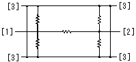
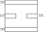
(1), (2) Input and output terminals (3) Ground terminals
|
<Specification>
|
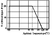
Type |
Graph 1 Derating Curve
|
||||
| Items | PAT3042 | PAT4556 | |||
| Impedance |
50O(C) |
||||
| Attenuation |
1,2,3,4,5,6,7,8,9,10,16,20dB |
||||
| VSWR | 1.1
(DC~2GHz) |
1.2
(2~5GHz) |
1.3 (5~10GHz) |
||
| Operating Frequency Range | DC~10GHz | ||||
| Rated Input Power (Derating Curve Graph 1) | 250mW | 500mW | |||
| Operating Temperature Range | -55°C~+125°C | ||||
| Rated Operating Temperature | 70°C | ||||
| Attenuation | Rank | DC~2GHz | 2~5GHz | 5~10GHz |
| 0dB | A | +0.1/-0dB | +0.2/-0dB | +0.4/-0dB |
| 1~10dB | A | ±0.1dB | ±0.2dB | ±0.4dB |
| B | ±0.2dB | ±0.3dB | ±0.5dB | |
| 16,20dB | B | ±0.2dB | ±0.3dB | ±0.5dB |
<Characteristics>
|
Items |
Test Condition | Tolerance | ||
| Attenuation | Impedance | |||
| 0~10dB |
16,20dB |
|||
| Short Time Over Load |
2.5 times of the rated voltage shall be applied for 5seconds. |
±0.01dB | ±0.02dB |
±0.2% |
| Load Life |
Apply rated voltage for 90 min followed by a pause of 30 min at 70±3°C for 1000 hours. |
±0.02dB | ±0.04dB | ±0.5% |
| Moisture Load Life |
The attenuator is applied rated voltage for 90 min followed by a pause of 30 min in 60±2°C and 90~95%RH for 1000 hours. |
±0.02dB | ±0.04dB | ±0.5% |
| Temperature Cycle |
[-55°C(30min)-R.T.(3min)-+125°C(30min)-R.T.(3min)]
is repeated 5 cycles. |
±0.01dB | ±0.02dB | ±0.2% |
| Solder Heat Resistance |
Leave attenuator in melt solder of 260±5°C for 10 ±1seconds. |
±0.01dB |
±0.02dB |
±0.2% |
| Strength between terminals |
Distance
between fulcrums :90mm
Bending
width :3mm Substrate :Glass epoxy t=1.6mm |
±0.01dB |
±0.02dB |
±0.2% |
| Solderbility |
Leave attenuator in melt solder of 235±5°C for 3±0.5 seconds. |
95% or more of the surface should be wet. | ||
| Insulation Resistance |
A minute after DC500V |
1000MO?? | ||
| Temperature Coefficient of Resistance |
R.T.---R.T.+100°C---R.T. |
±0.005 dB | ±0.01dB | ±50ppm/? |
<Taping>
For further information of packaging. CLICK!
|
Yokohama Densi Seiko Co., Ltd. |