|
PAT1220 |
||
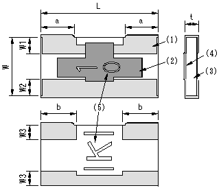 |
L | 2.0±0.1(mm) |
| W | 1.25±0.1(mm) | |
| t | 0.4±0.1(mm) | |
| a | 0.5±0.2(mm) | |
| b | 0.6±0.2(mm) | |
| W1 | 0.4±0.2(mm) | |
| W2 | 0.4±0.2(mm) | |
| W3 | 0.35±0.2(mm) | |
|
Chip Attenuator PAT series |
?
?
Surface mounting type Chip Attenuator PAT*** series
<Mechanical and Dimension>
|
PAT1220 |
||
|
L | 2.0±0.1(mm) |
| W | 1.25±0.1(mm) | |
| t | 0.4±0.1(mm) | |
| a | 0.5±0.2(mm) | |
| b | 0.6±0.2(mm) | |
| W1 | 0.4±0.2(mm) | |
| W2 | 0.4±0.2(mm) | |
| W3 | 0.35±0.2(mm) | |
| PAT1632 | ||
 |
L | 3.2±0.2(mm) |
| W | 1.6±0.2(mm) | |
| t | 0.4±0.1(mm) | |
| a | 1.0±0.25(mm) | |
| b | 1.0±0.2(mm) | |
| W1 | 0.55±0.25(mm) | |
| W2 | 0.4±0.25(mm) | |
| W3 | 0.4±0.2(mm) | |
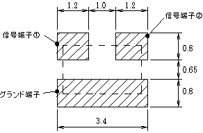
| PAT3042S | |||
 |
C(50O) | D(75O) | |
| L | 4.2±0.2(mm) | 4.2±0.2(mm) | |
| W | 3.0±0.2(mm) | 3.0±0.2(mm) | |
| t | 0.8±0.15(mm) | 0.8±0.15(mm) | |
| a | 0.8±0.2(mm) | 0.8±0.2(mm) | |
| b | 0.5±0.2(mm) | 0.3±0.2(mm) | |
| Lb | 3.1±0.2(mm) | 3.5±0.2(mm) | |
| W1 | 0.95±0.2(mm) | 0.55±0.2(mm) | |
| W2 | 0.8±0.2(mm) | 0.6±0.2(mm) | |
| Wa | 1.05±0.2(mm) | 1.55±0.2(mm) | |
| W3 | 0.95±0.2(mm) | 0.55±0.2(mm) | |
| W4 | 0.9±0.2(mm) | 0.6±0.2(mm) | |
| Wb | 0.95±0.2(mm) | 1.55±0.2(mm) | |
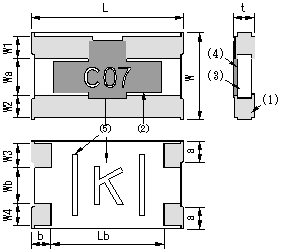
|
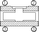
(1) |
Electrode (Surface soldering and lead-free possible) |
|
(2) |
Covering resin |
|
(3) |
Alumina substrate |
|
(4) |
Thin film resistor |
|
(5) |
Mark (shows impedance, attenuation and date) |
|
|
|
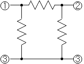
(1),(2) Input Terminals (3) Ground Terminals
|
<Specification>
| Items |
Types |
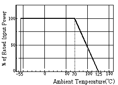
Graph 1 Derating Curve
|
|||
| PAT1220 | PAT1632 |
PAT3042S |
|||
| Impedance | 50O | 50O |
C(50O) |
D(75O) |
|
| Attenuation(dB) | 0,1,2,3,4,5,6,7,8,9,10 | 0,1,2,3,4,5,6,7,8,9,10,16 |
0,1,2,3,4,5,6,7 8,9,10,16,20 |
0,1,2,3,4,5,6,7 8,9,10,16,20 |
|
| Attenuation Tolerance |
±0.3dB |
±0.3dB:0~10dB ±0.5dB:16dB |
±0.3dB:0~10dB ±0.5dB:16·20dB |
||
| VSWR | 1.3 | 1.3 | 1.2 | 1.3 | |
| Operating Frequency Range | DC~10GHz | DC~3GHz | DC~3GHz | DC~2GHz | |
|
Rated Input Power (Derating Curve Graph 1) |
100mW | 125mW |
250mW |
||
| Operating Temperature Range | -55°C~+125°C | ||||
| Rated Operating Temperature | 70°C | ||||
<Characteristics>
|
Items |
Test Conditions | Tolerance Change | ||
| Attenuation (dB) |
Impedance(%) |
|||
|
PAT1220 PAT1632 |
PAT3042S | |||
| Short Time Over Load |
2.5 times of the rated voltage shall be applied for 5seconds. |
±0.02 |
±0.2 |
|
| Load Life |
Apply rated voltage for 90 min followed by a pause of 30 min at 70±3°C for 1000 hours. |
±0.04 |
±0.5 |
|
| Moisture Load Life |
The attenuator is applied rated voltage for 90 min followed by a pause of 30 min in 60±2°C and 90~95%RH for 1000 hours. |
±0.04 |
±0.5 |
|
| Temperature Cycle |
[-55°C(30min)-R.T.(3min)-+125°C(30min)-R.T.(3min)]
is repeated 5 cycles. |
±0.02 |
±0.2 |
|
| Solder Heat Resistance |
Leave attenuator in melt solder of 260±5°C for 10 ±1seconds. |
±0.02 |
±0.2 |
|
| Strength between terminals |
Distance
between fulcrums :90mm Bending
width :3mm Substrate :Glass epoxy t=1.6mm |
±0.02 |
±0.2 |
|
| Solderbility |
Leave attenuator in melt solder of 235±5°C for 3±0.5 seconds. |
95% or more of the surface should be wet. |
||
| Insulation Resistance |
A minute after DC500V |
1000MO | ||
| Temperature Coefficient of Resistance |
R.T.---R.T.+100°C---R.T. |
±0.005 | 50ppm/°C | 25ppm/°C |
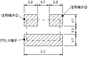
<Recommended
mounting pattern>
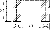
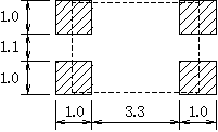
| PAT1220 | PAT1632 |
|
|
|
| PAT3042SC | PAT3042SD |
|
|
|
|
Note: Please take great care of frequency characteristics when deciding the width of wire from mounted part. |
<Taping>
For further information of taping. CLICK!
|
Yokohama Densi Seiko Co., Ltd. |